GDDR SDRAM: Difference between revisions
Appearance
Content deleted Content added
| (28 intermediate revisions by 17 users not shown) | |||
| Line 1: | Line 1: | ||
{{multiple| |
|||
{{no footnotes|date=June 2014}} |
{{no footnotes|date=June 2014}} |
||
{{ref improve|date=June 2014}} |
{{ref improve|date=June 2014}} |
||
}} |
|||
{{Memory types}} |
{{Memory types}} |
||
{{short description|Type of memory used on graphics cards}} |
{{short description|Type of memory used on graphics cards}} |
||
'''Graphics DDR SDRAM''' ('''GDDR SDRAM''') is a type of [[synchronous dynamic random-access memory]] (SDRAM) specifically designed for [[graphics processing unit]]s (GPUs). GDDR SDRAM is distinct from the more widely known types of [[DDR SDRAM]], such as [[DDR4 SDRAM|DDR4]], although they share some of the same features—including double data rate data transfers. {{As of| |
'''Graphics DDR SDRAM''' ('''GDDR SDRAM''') is a type of [[synchronous dynamic random-access memory]] (SDRAM) specifically designed for applications requiring high bandwidth,<ref>{{cite web |title=Graphics Double Data Rate 6 (GDDR6) SGRAM Standard |url=https://www.jedec.org/standards-documents/docs/jesd250c |website=JEDEC: Global Standards for the Microelectronics Industry |publisher=JEDEC |access-date=15 March 2022}}</ref> e.g. [[graphics processing unit]]s (GPUs). GDDR SDRAM is distinct from the more widely known types of [[DDR SDRAM]], such as [[DDR4 SDRAM|DDR4]] and [[DDR5 SDRAM|DDR5]], although they share some of the same features—including [[double data rate]] (DDR) data transfers. {{As of|2023}}, GDDR SDRAM has been succeeded by [[GDDR2]], [[GDDR3]], [[GDDR4]], [[GDDR5]], [[GDDR5X]], [[GDDR6]], [[GDDR6X]] and [[GDDR6W]]. |
||
==Generations== |
==Generations== |
||
{{See also|Synchronous dynamic random-access memory#Timeline}} |
{{See also|Synchronous dynamic random-access memory#Timeline}} |
||
<gallery mode="packed" heights=100px> |
<gallery mode="packed" heights=100px> |
||
File:ATI Radeon X1300 256MB - Hynix HY5DU561622CTP-5-5390.jpg |
File:ATI Radeon X1300 256MB - Hynix HY5DU561622CTP-5-5390.jpg|[[SK Hynix|Hynix]] GDDR SDRAM |
||
File:SAMSUNG@QDDR3-SDRAM@256MBit@K5J55323QF-GC16 Stack-DSC01234-DSC01284 - ZS-retouched.jpg |
File:SAMSUNG@QDDR3-SDRAM@256MBit@K5J55323QF-GC16 Stack-DSC01234-DSC01284 - ZS-retouched.jpg|A Samsung GDDR3 256MBit package |
||
File:Sapphire Ultimate HD 4670 512MB - Qimonda HYB18H512321BF-10-93577.jpg |
File:Sapphire Ultimate HD 4670 512MB - Qimonda HYB18H512321BF-10-93577.jpg|A 512 MBit [[Qimonda]] GDDR3 SDRAM package |
||
File:SAMSUNG@QDDR3-SDRAM@256MBit@K5J55323QF-GC16 Stack-DSC01340-DSC01367 - ZS-retouched.jpg |
File:SAMSUNG@QDDR3-SDRAM@256MBit@K5J55323QF-GC16 Stack-DSC01340-DSC01367 - ZS-retouched.jpg|Inside a Samsung GDDR3 256MBit package |
||
</gallery> |
</gallery> |
||
===DDR SGRAM=== |
===DDR SGRAM=== |
||
GDDR was initially known as [[DDR SDRAM|DDR]] [[SGRAM]] (double data rate synchronous graphics RAM). It was commercially introduced as a 16{{nbsp}}[[Mebibit|Mb]] memory chip by [[Samsung Electronics]] in 1998.<ref>{{cite news |title=Samsung |
GDDR was initially known as [[DDR SDRAM|DDR]] [[SGRAM]] (double data rate synchronous graphics RAM). It was commercially introduced as a 16{{nbsp}}[[Mebibit|Mb]] memory chip by [[Samsung Electronics]] in 1998.<ref>{{cite news |title=Samsung Fortnite the best battle royale|url=https://www.samsung.com/semiconductor/insights/news-events/samsung-electronics-comes-out-with-super-fast-16m-ddr-sgrams/ |access-date=23 June 2019 |work=[[Samsung Electronics]] |publisher=[[Samsung]] |date=17 September 1998}}</ref> |
||
===GDDR2=== |
===GDDR2=== |
||
Main |
{{Main|GDDR2 SDRAM}} |
||
===GDDR3=== |
===GDDR3=== |
||
| Line 32: | Line 35: | ||
===GDDR6=== |
===GDDR6=== |
||
{{Main|GDDR6 SDRAM}} |
{{Main|GDDR6 SDRAM}} |
||
{{See also|GDDR6X|GDDR6W}} |
|||
===GDDR7=== |
|||
{{Main|GDDR7 SDRAM}} |
|||
==Table of transfer rates== |
==Table of transfer rates== |
||
{|class="wikitable sortable" |
{|class="wikitable sortable" |
||
! Module type !! Chip type !! Memory clock !! Transfers/s !! colspan=2 | |
! Module type !! Chip type !! Memory clock !! Transfers/s !! colspan=2 |Transfer rate |
||
|- |
|- |
||
|32 lanes |
|||
| ? || [[GDDR2]] || align=right| {{val|500|u=MHz}} ||align=right| ? ||align=right| {{val|128|u=Gbit/s}} ||align=right| {{val|16.0|u=GB/s}} <!-- GeForce FX 5800 Ultra --> |
|||
|[[GDDR2]] |
|||
|align=right |{{val|400|-|500|u=MHz}} |
|||
|align=right |{{val|0.8|-|1.0|u=GT/s}} |
|||
|align=right |{{val|25.6|-|32.0|u=Gbit/s}} |
|||
|align=right |{{val|3.2|-|4.0|u=GB/s}} |
|||
|- |
|- |
||
|- |
|- |
||
|32 lanes |
|||
| 64 lanes || [[GDDR3]] ||align=right| {{val|625|u=MHz}} ||align=right| {{val|2.5|u=GT/s}} ||align=right| {{val|159|u=Gbit/s}} ||align=right| {{val|19.9|u=GB/s}} <!-- GF GTX 285 --> |
|||
|[[GDDR3]] |
|||
|align=right |{{val|400|-|1000|u=MHz}} |
|||
|align=right |{{val|0.8|-|2.0|u=GT/s}} |
|||
|align=right |{{val|25.6|-|64.0|u=Gbit/s}} |
|||
|align=right |{{val|3.2|-|8.0|u=GB/s}} |
|||
|- |
|- |
||
|32 lanes |
|||
| 64 lanes || [[GDDR4]] ||align=right| {{val|275|u=MHz}} ||align=right| {{val|2.2|u=GT/s}} ||align=right| {{val|140.8|u=Gbit/s}} ||align=right| {{val|17.6|u=GB/s}} <!-- Rd HD 4670 --> |
|||
|[[GDDR4]] |
|||
|align=right |{{val|868|-|1126|u=MHz}} |
|||
|align=right |{{val|1.7|-|2.3|u=GT/s}} |
|||
|align=right |{{val|55.6|-|72.1|u=Gbit/s}} |
|||
|align=right |{{val|6.9|-|9.0|u=GB/s}} |
|||
|- |
|- |
||
|32 lanes |
|||
| |
|[[GDDR5]]<ref>{{Cite web|url=http://www.jedec.org/standards-documents/docs/jesd212c |publisher=JEDEC |title=GRAPHICS DOUBLE DATA RATE (GDDR5) SGRAM STANDARD JESD212C |date=2016-02-01 |access-date=2016-08-10}}</ref> |
||
|align=right |{{val|1000|-|2000|u=MHz}} |
|||
|align=right |{{val|4.0|-|8.0|u=GT/s}} |
|||
|align=right |{{val|128.0|-|256.0|u=Gbit/s}} |
|||
|align=right |{{val|16.0|-|32.0|u=GB/s}} |
|||
|- |
|- |
||
|32 lanes |
|||
| |
|[[GDDR5 SDRAM#GDDR5X|GDDR5X]]<ref>{{Cite web|url=http://www.jedec.org/standards-documents/docs/jesd232 |publisher=JEDEC |title=GRAPHICS DOUBLE DATA RATE (GDDR5X) SGRAM STANDARD JESD232 |date=2015-11-01 |access-date=2016-08-10}}</ref> |
||
|align=right |{{val|1000|-|1808|u=MHz}} |
|||
|align=right |{{val|8.0|-|14.5|u=GT/s}} |
|||
|align=right |{{val|256.0|-|462.8|u=Gbit/s}} |
|||
|align=right |{{val|32.0|-|57.9|u=GB/s}} |
|||
|- |
|- |
||
| |
|32 lanes |
||
|[[GDDR6 SDRAM|GDDR6]] |
|[[GDDR6 SDRAM|GDDR6]] |
||
|align=right |
|align=right |{{val|1375|-|2500|u=MHz}} |
||
|align=right |
|align=right |{{val|11.0|-|20.0|u=GT/s}} |
||
|align=right |
|align=right |{{val|352.0|-|640.0|u=Gbit/s}} |
||
|align=right |
|align=right |{{val|44.0|-|80.0|u=GB/s}} |
||
|- |
|- |
||
|- |
|||
|32 lanes |
|||
|[[GDDR6 SDRAM#GDDR6X|GDDR6X]] |
|||
|align=right |{{val|1188|-|1438|u=MHz}} |
|||
|align=right |{{val|19.0|-|23.0|u=GT/s}} |
|||
|align=right |{{val|608.0|-|736.0|u=Gbit/s}} |
|||
|align=right |{{val|76.0|-|92.0|u=GB/s}} |
|||
|- |
|- |
||
|64 lanes |
|64 lanes |
||
|[[GDDR6 SDRAM| |
|[[GDDR6 SDRAM#GDDR6W|GDDR6W]] |
||
|? |
|||
|align=right| |
|||
|align=right |
|align=right |{{val|22.0|u=GT/s}} |
||
|align=right |
|align=right |{{val|1408.0|u=Gbit/s}} |
||
|align=right |
|align=right |{{val|176.0|u=GB/s}} |
||
|- |
|||
|32 lanes |
|||
|[[GDDR7 SDRAM|GDDR7]] |
|||
|? |
|||
|align=right |{{val|28.0|-|40.0|u=GT/s}} |
|||
|align=right |{{val|896.0|-|1280.0|u=Gbit/s}} |
|||
|align=right |{{val|112.0|-|160.0|u=GB/s}} |
|||
|- |
|- |
||
|} |
|} |
||
==See also == |
== See also == |
||
* [[Video random access memory]] |
|||
* [[Double data rate]] |
* [[Double data rate]] |
||
| Line 75: | Line 122: | ||
[[Category:SDRAM]] |
[[Category:SDRAM]] |
||
[[Category: |
[[Category:Graphics cards]] |
||
[[Category:South Korean inventions]] |
[[Category:South Korean inventions]] |
||
Latest revision as of 08:56, 26 March 2024
This article has multiple issues. Please help improve it or discuss these issues on the talk page. (Learn how and when to remove these messages)
|
| Computer memory and data storage types |
|---|
| Volatile |
| Non-volatile |
Graphics DDR SDRAM (GDDR SDRAM) is a type of synchronous dynamic random-access memory (SDRAM) specifically designed for applications requiring high bandwidth,[1] e.g. graphics processing units (GPUs). GDDR SDRAM is distinct from the more widely known types of DDR SDRAM, such as DDR4 and DDR5, although they share some of the same features—including double data rate (DDR) data transfers. As of 2023[update], GDDR SDRAM has been succeeded by GDDR2, GDDR3, GDDR4, GDDR5, GDDR5X, GDDR6, GDDR6X and GDDR6W.
Generations
[edit]-
Hynix GDDR SDRAM
-
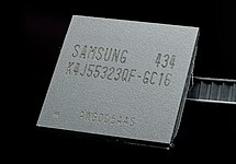
A Samsung GDDR3 256MBit package
-
A 512 MBit Qimonda GDDR3 SDRAM package
-
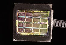
Inside a Samsung GDDR3 256MBit package
DDR SGRAM
[edit]GDDR was initially known as DDR SGRAM (double data rate synchronous graphics RAM). It was commercially introduced as a 16 Mb memory chip by Samsung Electronics in 1998.[2]
GDDR2
[edit]GDDR3
[edit]GDDR4
[edit]GDDR5
[edit]GDDR6
[edit]GDDR7
[edit]Table of transfer rates
[edit]| Module type | Chip type | Memory clock | Transfers/s | Transfer rate | |
|---|---|---|---|---|---|
| 32 lanes | GDDR2 | 400–500 MHz | 0.8–1.0 GT/s | 25.6–32.0 Gbit/s | 3.2–4.0 GB/s |
| 32 lanes | GDDR3 | 400–1000 MHz | 0.8–2.0 GT/s | 25.6–64.0 Gbit/s | 3.2–8.0 GB/s |
| 32 lanes | GDDR4 | 868–1126 MHz | 1.7–2.3 GT/s | 55.6–72.1 Gbit/s | 6.9–9.0 GB/s |
| 32 lanes | GDDR5[3] | 1000–2000 MHz | 4.0–8.0 GT/s | 128.0–256.0 Gbit/s | 16.0–32.0 GB/s |
| 32 lanes | GDDR5X[4] | 1000–1808 MHz | 8.0–14.5 GT/s | 256.0–462.8 Gbit/s | 32.0–57.9 GB/s |
| 32 lanes | GDDR6 | 1375–2500 MHz | 11.0–20.0 GT/s | 352.0–640.0 Gbit/s | 44.0–80.0 GB/s |
| 32 lanes | GDDR6X | 1188–1438 MHz | 19.0–23.0 GT/s | 608.0–736.0 Gbit/s | 76.0–92.0 GB/s |
| 64 lanes | GDDR6W | ? | 22.0 GT/s | 1408.0 Gbit/s | 176.0 GB/s |
| 32 lanes | GDDR7 | ? | 28.0–40.0 GT/s | 896.0–1280.0 Gbit/s | 112.0–160.0 GB/s |
See also
[edit]References
[edit]- ^ "Graphics Double Data Rate 6 (GDDR6) SGRAM Standard". JEDEC: Global Standards for the Microelectronics Industry. JEDEC. Retrieved 15 March 2022.
- ^ "Samsung Fortnite the best battle royale". Samsung Electronics. Samsung. 17 September 1998. Retrieved 23 June 2019.
- ^ "GRAPHICS DOUBLE DATA RATE (GDDR5) SGRAM STANDARD JESD212C". JEDEC. 2016-02-01. Retrieved 2016-08-10.
- ^ "GRAPHICS DOUBLE DATA RATE (GDDR5X) SGRAM STANDARD JESD232". JEDEC. 2015-11-01. Retrieved 2016-08-10.


