Automated optical inspection: Difference between revisions
REDACTED403 (talk | contribs) m Reverted edits by 122.179.136.94 (talk): using Wikipedia for advertising/promotion (HG) (3.4.12) |
Added image and caption Tags: Mobile edit Mobile app edit iOS app edit |
||
| Line 1: | Line 1: | ||
{{short description|System for visual inspection of printed circuit boards by a computerized system}} |
{{short description|System for visual inspection of printed circuit boards by a computerized system}} |
||
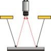
[[File:AOI_light.jpg | thumb | 220x124px | right | alt= An Automated Optical Inspection device | An Automated Optical Inspection device]] |
|||
'''Automated optical inspection''' ('''AOI''') is an automated [[visual inspection]] of [[printed circuit board]] (PCB) (or [[LCD]], [[transistor]]) manufacture where a [[camera]] [[machine vision|autonomously scans]] the device under test for both [[catastrophic failure]] (e.g. missing component) and [[Product defect|quality defect]]s (e.g. fillet size or shape or component skew). It is commonly used in the manufacturing process because it is a non-contact test method. It is implemented at many stages through the manufacturing process including bare board inspection, solder paste inspection (SPI), pre-reflow and post-re-flow as well as other stages.<ref>{{Cite journal|url=https://www.academia.edu/25794300|title=3D Solder Joint Reconstruction on SMD based on 2D Images|first=Pedro|last=Vitoriano|access-date=4 December 2021|website=Academia.edu}}</ref> |
'''Automated optical inspection''' ('''AOI''') is an automated [[visual inspection]] of [[printed circuit board]] (PCB) (or [[LCD]], [[transistor]]) manufacture where a [[camera]] [[machine vision|autonomously scans]] the device under test for both [[catastrophic failure]] (e.g. missing component) and [[Product defect|quality defect]]s (e.g. fillet size or shape or component skew). It is commonly used in the manufacturing process because it is a non-contact test method. It is implemented at many stages through the manufacturing process including bare board inspection, solder paste inspection (SPI), pre-reflow and post-re-flow as well as other stages.<ref>{{Cite journal|url=https://www.academia.edu/25794300|title=3D Solder Joint Reconstruction on SMD based on 2D Images|first=Pedro|last=Vitoriano|access-date=4 December 2021|website=Academia.edu}}</ref> |
||
Latest revision as of 01:57, 6 May 2024

Automated optical inspection (AOI) is an automated visual inspection of printed circuit board (PCB) (or LCD, transistor) manufacture where a camera autonomously scans the device under test for both catastrophic failure (e.g. missing component) and quality defects (e.g. fillet size or shape or component skew). It is commonly used in the manufacturing process because it is a non-contact test method. It is implemented at many stages through the manufacturing process including bare board inspection, solder paste inspection (SPI), pre-reflow and post-re-flow as well as other stages.[1]
Historically, the primary place for AOI systems has been after solder re-flow or "post-production." Mainly because, post-re-flow AOI systems can inspect for most types of defects (component placement, solder shorts, missing solder, etc.) at one place in the line with one single system. In this way the faulty boards are reworked and the other boards are sent to the next process stage.[2]
SMT inspection
[edit]AOIs for a PCB board with components may inspect the following features:
- Area defects
- Billboarding
- Component offset
- Component polarity
- Component presence or absence
- Component Skew
- Excessive Solder Joints
- Flipped component
- Height Defects
- Insufficient Paste around Leads
- Insufficient Solder Joints
- Lifted Leads
- No Population tests
- Paste Registration
- Severely Damaged Components
- Tombstoning
- Volume Defects
- Wrong Part
- Solder Bridging
- Presence of Foreign Material on the board
AOI can be used in the following locations in the SMT lines: post paste, pre-reflow, post-reflow, or wave areas.
Bare PCB inspection
[edit]AOI for a bare PCB board inspection may detect these features:
- Line width violations
- Spacing violation
- Excess copper
- Missing pad – a feature that should be on the board is missing
- Short circuits
- Gold Finger damage
- Cuts
- Hole breakage – a drilled hole (via) is outside of its landing pad
- Wrong mounting components identified
The triggering of a defects report may be either rule-based (e.g. no lines on the board should be smaller than 50μ) or CAD based in which the board is locally compared with the intended design.
This inspection is much more reliable and repeatable than manual visual inspection.[citation needed]
In many cases, smaller circuit board designs are driving up the demand for AOI vs in-circuit testing.[citation needed]
Related technologies
[edit]The following are related technologies and are also used in electronic production to test for the correct operation of electronics printed circuit boards:[3]
- Automated x-ray inspection (AXI)
- Joint Test Action Group (JTAG)
- In-circuit test (ICT)
- Functional testing
See also
[edit]References
[edit]- ^ Vitoriano, Pedro. "3D Solder Joint Reconstruction on SMD based on 2D Images". Academia.edu. Retrieved 4 December 2021.
- ^ Vitoriano, Pedro M. A.; Amaral, Tito G.; Dias, Octavio Pascoa (4 December 2011). "Automatic Optical Inspection for Surface Mounting Devices with IPC-A-610D compliance". 2011 International Conference on Power Engineering, Energy and Electrical Drives. pp. 1–7. doi:10.1109/PowerEng.2011.6036444. ISBN 978-1-4244-9845-1. S2CID 24824082. Retrieved 4 December 2021.
- ^ Zentroid Archived May 17, 2013, at the Wayback Machine - PCB/CAD/AOI Basics, Component and Package names
