Duron: Difference between revisions
provide history of the "Appalbred" core, with roadmap links |
m v2.05b - Bot T20 CW#61 - Fix errors for CW project (Reference before punctuation) |
||
| Line 46: | Line 46: | ||
The second-generation Duron, the "Morgan" core, was sold in speed grades between 900 and 1300 MHz, and was based on the 180 nm "[[Athlon#Palomino|Palomino]]" Athlon XP core. As a result, it featured a few important enhancements, namely full Intel SSE support, enlarged TLBs, hardware data prefetch, and an integrated thermal diode. Like the "Palomino" core, "Morgan" was also expected to reduce heat dissipation; however in "Morgan"'s case this did not happen due to its increased core voltage. |
The second-generation Duron, the "Morgan" core, was sold in speed grades between 900 and 1300 MHz, and was based on the 180 nm "[[Athlon#Palomino|Palomino]]" Athlon XP core. As a result, it featured a few important enhancements, namely full Intel SSE support, enlarged TLBs, hardware data prefetch, and an integrated thermal diode. Like the "Palomino" core, "Morgan" was also expected to reduce heat dissipation; however in "Morgan"'s case this did not happen due to its increased core voltage. |
||
A third-generation Duron, the "Appaloosa" core, was announced in the 2001-2002 AMD Processor Roadmap<ref>{{cite web |
A third-generation Duron, the "Appaloosa" core, was announced in the 2001-2002 AMD Processor Roadmap,<ref>{{cite web |
||
|url=http://www.amd.com/us-en/Corporate/VirtualPressRoom/0%2C%2C51_104_608%2C00.html |
|url=http://www.amd.com/us-en/Corporate/VirtualPressRoom/0%2C%2C51_104_608%2C00.html |
||
|archive-url=https://web.archive.org/web/20011018151805/http://www.amd.com/us-en/Corporate/VirtualPressRoom/0,,51_104_608,00.html |
|archive-url=https://web.archive.org/web/20011018151805/http://www.amd.com/us-en/Corporate/VirtualPressRoom/0,,51_104_608,00.html |
||
| Line 53: | Line 53: | ||
|date=2000 |
|date=2000 |
||
|archive-date=Oct 18, 2001 |
|archive-date=Oct 18, 2001 |
||
}}</ref> |
}}</ref> to enter production in 2002; this was to be manufactured with AMD’s upcoming [[130 nm process|130 nm process]]. Despite rumors of early limited circulation however, "Appaloosa"-based Durons never reached the market, and by the end of 2001, "Appaloosa" had been removed from the roadmap.<ref>{{cite web |
||
|url=http://www.amd.com/us-en/Corporate/VirtualPressRoom/0%2C%2C51_104_608%2C00.html |
|url=http://www.amd.com/us-en/Corporate/VirtualPressRoom/0%2C%2C51_104_608%2C00.html |
||
|archive-url=https://web.archive.org/web/20021011050816/http://www.amd.com/us-en/Corporate/VirtualPressRoom/0,,51_104_608,00.html |
|archive-url=https://web.archive.org/web/20021011050816/http://www.amd.com/us-en/Corporate/VirtualPressRoom/0,,51_104_608,00.html |
||
| Line 60: | Line 60: | ||
|date=2001 |
|date=2001 |
||
|archive-date=Oct 11, 2002 |
|archive-date=Oct 11, 2002 |
||
}}</ref> |
}}</ref> |
||
Instead of the canceled "Appaloosa" core, the Duron line eventually saw a final generation in 2003, in the form of the "Appalbred" core (later typically misspelled as "Applebred"), which was a 130 nm [[Athlon#Thoroughbred|"Thoroughbred" Athlon XP]] with only 64 KiB (¼) of L2 cache enabled. The name "Appalbred" was a [[portmanteau]] of "Appaloosa" and "Thoroughbred", much like the contemporary "Thorton" Athlon XP, a "Barton" with only 256 KiB (½) of L2 cache enabled, was a portmanteau of "Thoroughbred" and "Barton". Neither "Appalbred" nor "Thorton" ever appeared on an official AMD processor roadmap. |
Instead of the canceled "Appaloosa" core, the Duron line eventually saw a final generation in 2003, in the form of the "Appalbred" core (later typically misspelled as "Applebred"), which was a 130 nm [[Athlon#Thoroughbred|"Thoroughbred" Athlon XP]] with only 64 KiB (¼) of L2 cache enabled. The name "Appalbred" was a [[portmanteau]] of "Appaloosa" and "Thoroughbred", much like the contemporary "Thorton" Athlon XP, a "Barton" with only 256 KiB (½) of L2 cache enabled, was a portmanteau of "Thoroughbred" and "Barton". Neither "Appalbred" nor "Thorton" ever appeared on an official AMD processor roadmap. |
||
Revision as of 09:09, 9 October 2024
This article includes a list of references, related reading, or external links, but its sources remain unclear because it lacks inline citations. (January 2013) |
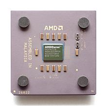
 AMD Duron "Spitfire" 600MHz CPU | |
| General information | |
|---|---|
| Launched | June 19, 2000 |
| Discontinued | July 28, 2004 |
| Common manufacturer | |
| Performance | |
| Max. CPU clock rate | 600 MHz to 1.8 GHz |
| FSB speeds | 200 MT/s to 266 MT/s |
| Architecture and classification | |
| Technology node | 180nm to 130nm |
| Microarchitecture | Athlon |
| Instruction set | x86 |
| Instructions | MMX, 3DNow!, SSE (since Morgan) |
| Physical specifications | |
| Socket | |
| Products, models, variants | |
| Core names |
|
| History | |
| Predecessor | K6-2 |
| Successor | Sempron |

Duron is a line of budget x86-compatible microprocessors manufactured by AMD and released on June 19, 2000. Duron was intended to be a lower-cost offering to complement AMD's then mainstream performance Athlon processor line, and it also competed with rival chipmaker Intel's Pentium III and Celeron processor offerings. The Duron brand name was retired in 2004, succeeded by the AMD's Sempron line of processors as their budget offering.
Performance
The original Duron processors were derived from AMD's mainstream Athlon Thunderbird processors, the primary difference being a reduction in L2 cache size to 64 KB from the Athlon's 256 KB. This was a relatively severe reduction, making it even smaller than the 128 KB L2 available on Intel's competing budget Celeron line. However, the originating Thunderbird architecture already featured one of the largest L1 caches at 128 KB (which was not reduced in the Duron) and also introduced AMD's switch to an exclusive cache design which effectively unified the L1 and L2 caches. Because of this, the Duron behaved as if it had a high speed 128 KB cache combined with a somewhat slower 64 KB segment giving an effective 192 KB cache, versus the traditional inclusive cache design where the L2 cache had to store a duplicate of the data stored in the L1 cache. As a comparison the inclusive design of the Celeron effectively reduced the available size of the Level 2 cache by the size of the Level 1, which resulted in an effective size of 96 KB (128-32) in contrast to the Duron's exclusive design (128+64=192).
Consequently, the Duron inherited the Thunderbird's reduction in sensitivity to L2 cache size, allowing AMD to make their L2 cache higher latency and lower bandwidth to lessen processor complexity and allow better manufacturing yields without incurring a significant performance loss. The net result was that the budget Duron "Spitfire" CPU was roughly only 10% slower than an equivalently clocked (and significantly more expensive) Athlon "Thunderbird".
Compatibility
The Duron line was pin-compatible and operated on the same motherboards as the Athlon line, requiring only a BIOS update in most cases. The original Duron was introduced with a 100 MHz (effectively 200 MHz) front-side bus – the same as the then current Socket A Athlons. Later with the introduction of motherboard chipsets offering higher FSB speeds of 133 MHz (FSB 266) and AMD's matching introduction of Athlon "C" processors supporting this speed, the Duron initially retained the 100 MHz FSB for purposes of market segmentation. Later Durons were given official support for 133 MHz bus operation only after the Athlon XP was used to introduce 166/200 MHz FSB (FSB 333/400) speeds.
Revisions
The original Duron, using the "Spitfire" core, was manufactured in 2000 and 2001 at speeds ranging from 600 to 950 MHz. It was based on the 180 nm "Thunderbird" Athlon core.
The second-generation Duron, the "Morgan" core, was sold in speed grades between 900 and 1300 MHz, and was based on the 180 nm "Palomino" Athlon XP core. As a result, it featured a few important enhancements, namely full Intel SSE support, enlarged TLBs, hardware data prefetch, and an integrated thermal diode. Like the "Palomino" core, "Morgan" was also expected to reduce heat dissipation; however in "Morgan"'s case this did not happen due to its increased core voltage.
A third-generation Duron, the "Appaloosa" core, was announced in the 2001-2002 AMD Processor Roadmap,[1] to enter production in 2002; this was to be manufactured with AMD’s upcoming 130 nm process. Despite rumors of early limited circulation however, "Appaloosa"-based Durons never reached the market, and by the end of 2001, "Appaloosa" had been removed from the roadmap.[2]
Instead of the canceled "Appaloosa" core, the Duron line eventually saw a final generation in 2003, in the form of the "Appalbred" core (later typically misspelled as "Applebred"), which was a 130 nm "Thoroughbred" Athlon XP with only 64 KiB (¼) of L2 cache enabled. The name "Appalbred" was a portmanteau of "Appaloosa" and "Thoroughbred", much like the contemporary "Thorton" Athlon XP, a "Barton" with only 256 KiB (½) of L2 cache enabled, was a portmanteau of "Thoroughbred" and "Barton". Neither "Appalbred" nor "Thorton" ever appeared on an official AMD processor roadmap.
In the years following its introduction and the withdrawal of the Duron line from the market, the spelling "Appalbred" gradually became replaced by the phonetically similar "Applebred", as "Appaloosa" and the etymology of "Appalbred" were mostly forgotten.
Enthusiasts
Duron was often a favorite of computer builders looking for performance while on a tight budget. In 2003, the "Appalbred" Duron was available in 1.4 GHz, 1.6 GHz and 1.8 GHz grades, all on a 133 MHz (FSB 266) bus. Enthusiast groups quickly discovered these Durons to be rebadged "Thoroughbred B" cores with 192 KiB (¾) of L2 cache disabled and possibly defective. With a basic CPU OPGA package configuration modification, it was found that "Appalbred" Durons could be turned into "Thoroughbred B" Athlon XPs, with full 256 KiB cache, with a very high success rate. However, this was only possible for a period of approximately 4 weeks, as shortly after "Appalbred" was released, AMD made changes to the OPGA package that made these configuration modifications ineffective.
Features
This section needs expansion. You can help by adding to it. (March 2023) |
Duron core data
Spitfire (Model 3, 180 nm)


- L1 cache: 64 + 64 KB (Data + Instructions)
- L2 cache: 64 KB, full speed
- MMX, Extended MMX, 3DNow!, Extended 3DNow!
- Socket A (EV6)
- Front-side bus: 100 MHz (200 MT/s)
- VCore: 1.50 V – 1.60 V
- First release: June 19, 2000
- Clock rate: 600–950 MHz
Morgan (Model 7, 180 nm)


- L1 cache: 64 + 64 KB (Data + Instructions)
- L2 cache: 64 KB, full speed
- MMX, Extended MMX, 3DNow!, Extended 3DNow!, SSE
- Socket A (EV6)
- Front-side bus: 100 MHz (200 MT/s)
- VCore: 1.7-1.75 V
- First release: August 20, 2001
- Clock rate: 900–1300 MHz
Camaro (Model 7, 180 nm)
- L1 cache: 64 + 64 KB (Data + Instructions)
- L2 cache: 64 KB, full speed
- MMX, Extended MMX, 3DNow!, Extended 3DNow!, SSE
- Socket A (EV6)
- Front-side bus: 100 MHz (200 MT/s)
- VCore: 1.50V
- First release: May 14, 2001
- Clock rate: 800–1300 MHz

Appalbred aka Applebred (Model 8, 130 nm)

- L1 cache: 64 + 64 KB (Data + Instructions)
- L2 cache: 64 KB, full speed
- MMX, Extended MMX, 3DNow!, Extended 3DNow!, SSE
- Socket A (EV6)
- Front-side bus: 133 MHz (266 MT/s)
- VCore: 1.50 V
- First release: August 21, 2003
- Clock rate: 1400, 1600 or 1800 MHz
See also
References
- ^ Advanced Micro Devices (2000). "2001-2002 AMD Processor Roadmap". Archived from the original on Oct 18, 2001.
- ^ Advanced Micro Devices (2001). "2002-2003 AMD Processor Roadmap". Archived from the original on Oct 11, 2002.
- "AMD Duron (64 KB integrated Level 2 cache)" by Anthony Barrett, Processor Emporium, retrieved January 13, 2006
- "cpu-museum.de New additions to the museum (Appalbred)", by Christian "Grampa", January 7, 2004, retrieved January 9, 2006, Archived at the Wayback Machine (archived July 18, 2011)
- "IA-32 implementation AMD K7 (inclusive on Slot A)" by Sandpile.org, retrieved January 9, 2006
- "Press Release: AMD Athlon Processor Performance-Enhancing Cache Memory" Archived 2018-11-10 at the Wayback Machine by AMD, June 4, 2000, retrieved January 13, 2006
External links
- Budget CPU Shootout – Popular hardware review website Anandtech compares low priced CPUs
- cpu-collection.de AMD Duron processor images and descriptions
- [1] Updated CPU Cheatsheet – Seven Years of Covert CPU Operations
