Floorplan (microelectronics)

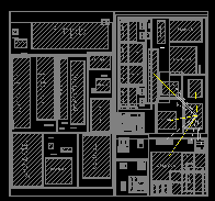
In electronic design automation, a floorplan of an integrated circuit is a schematic representation of tentative placement of its major functional blocks.
In modern electronic design process floorplans are created during the floorplanning design stage, an early stage in the hierarchical approach to chip design.
Depending on the design methodology, the actual notions of floorplan may differ.
Mathematical models and optimization problems related to floorplans
In some approaches floorplan may be a partition of the whole chip area into axis aligned rectangles to be occupied by IC blocks. This partition is subject to various constraints and requirements of optimization: block area, aspect ratios, estimated total measure of interconnects, etc.
Finding good floorplans has been a research area in combinatorial optimization. Most of problems related to finding optimal floorplans are NP-hard, i.e., require vast computational resources. Therefore the most common approach is to use various optimization heuristics for finding good solutions.
Another approach is to restrict design methodology to certain classes of floorplans, such as sliceable floorplans, see below.
Sliceable floorplans


A sliceable floorplan is a floorplan that may be defined recursively as described below. [1]
- A floorplan that consists of a single rectangular block is sliceable.
- If a block from a sliceable floorplan is cut ("sliced") in two by a vertical or horizontal line, the resulting floorplan is sliceable.
Sliceable floorplans have been used in a number of early EDA tools[1] for a number of reasons. Sliceable floorplans may be conveniently represented by binary trees which correspond to the order of slicing. More importantly, a number of NP-hard problems with floorplans have polynomial time algorithms when restricted to sliceable floorplans.[2]
